3D Printing for Electronics Enclosures and Hardware Products
3D Printing for Electronics Enclosures and Hardware Products
Electronics teams use 3D printing to check PCB fit, prove enclosure lids, test button panels, trial snap fits and bridge low-volume hardware before tooling.

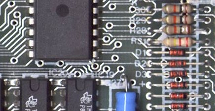
Photo: Macro view of a circuit board. Credit: Ingo Dierking / Wikimedia Commons (CC BY SA 4.0).
In this article
Electronics enclosures look simple until the real board, connectors, cables, buttons, labels and fasteners arrive. A millimetre of connector clash can delay a launch, and a screw boss that cracks during assembly can force a housing redesign. 3D printing catches those risks early.
Solidium3D prints enclosure lids, PCB fit-check housings, button panels, sensor shells and low-volume hardware for Australian product teams. FDM lead times are typically 2 to 5 business days. SLA lead times are typically 10 to 15 business days for high detail resin appearance models.
The objective is to produce an engineering sample that can verify fit, access, assembly sequence, fasteners, seals and serviceability—not only external appearance. A useful print proves board clearance, user access, assembly sequence, gasket strategy and whether the product can be serviced without damage.
PCB Fit-Checks Before Tooling
A printed enclosure should be assembled with the real PCB as early as possible. Board thickness, connector height, antenna space, heat sinks, cable bend radius and screw access can all change the housing. These issues are cheap to correct before tooling and expensive after.
CAD keep out zones help, but physical assembly reveals details that models often miss. The cable may need more room at the hinge side, the USB connector may sit off centre, or a service technician may need a different tool angle.
FDM is often best for fast functional checks because ABS, ASA and PETG parts can be handled, drilled and assembled. For suitable batch-production projects, SLA is useful when the team needs a smoother appearance model or fine details around buttons and light pipes.
 |
Board and Housing Need to be Reviewed TogetherA housing prototype without the real PCB is only a shape study. A better review includes the board, connectors, screws, labels, seals and cable exits. Ask for critical faces and holes to be identified in the quote notes so the manufacturing approach can protect the features that matter most. |
Bosses, Snap Fits, Lids and Button Panels
Screw bosses need enough wall around the fastener and enough base support to avoid splitting. For repeated assembly, heat-set inserts, captive nuts or through bolts are usually more reliable than printed threads.
Snap fits need controlled strain. Long clips with radii and assembly lead ins perform better than short rigid tabs with sharp roots. Printed prototypes are useful because the team can adjust clearance, length and engagement after real assembly tests.
Button panels and light pipe areas often favour SLA because small edges and smooth surfaces matter. For functional lids and larger housings, FDM ABS or ASA can provide a stronger practical prototype and a possible low-volume production bridge.

Photo: Electrical engineering laboratory for hardware development context. Credit: Aalto University Library and Archive Commons / Wikimedia Commons (No restrictions).
Production Bridge Strategies
Many hardware products need a small batch before tooling. Printed enclosures can serve pilot builds, field trials, test equipment, industrial devices and sales samples when tooling is not justified yet. The design should be simplified for repeatable assembly, not only for the first prototype.
EMI considerations should be discussed early. A printed plastic enclosure is not a shield by itself, so teams may need internal coatings, metal inserts, gasket features or a separate conductive strategy depending on the product.
TPU can be used for prototype gaskets, pads and flexible contact features, but sealing performance must be tested in the final assembly. Keeping the rigid housing and flexible gasket as separate functions often makes the design easier to test and revise.
Specification and Ordering Checklist
Electronics quote requests should include the board model or at least a clear connector drawing. The enclosure cannot be judged in isolation from the hardware inside it.
- Include PCB files, connector keep out zones and cable bend requirements.
- Use FDM ABS, ASA or PETG for functional lids and housings in 2 to 5 business days.
- Use SLA for smooth button panels, light pipe details and appearance models with 10 to 15 business days planned.
- Design bosses for inserts, captive nuts or through bolts if repeated assembly is expected.
- Document EMI, sealing, heat and label requirements before ordering a pilot batch.
Process Comparison
| Electronics requirement | Recommended route | Reason |
|---|---|---|
| PCB fit-check housing | FDM ABS, ASA or PETG | Fast functional assembly with real boards |
| Appearance front panel | SLA resin | Smooth surface and fine feature definition |
| Low volume industrial enclosure | FDM with inserts or SLS for compact nylon parts | Production bridge before tooling or for limited demand |
| Seal or gasket feature | Separate TPU gasket with rigid body | Keeps flexible sealing independent from housing stiffness |
FAQ
Can a printed electronics enclosure be used for a pilot batch?
Yes for suitable low-volume hardware when material, assembly method and service conditions are validated by the customer.
Should I use FDM or SLA for an enclosure?
Use FDM for functional structure and fast fit-checks. Use SLA for suitable batch-production projects when surface finish, button detail or presentation appearance is the priority.
Can 3D printing solve EMI shielding?
A standard printed polymer enclosure does not provide reliable EMI shielding by itself. Discuss coatings, inserts, gaskets or a separate shielding strategy if EMI is a requirement.
What lead time should hardware teams plan for?
FDM is typically 2 to 5 business days. SLA and SLS are typically 10 to 15 business days.
Related Reading

Material and process guidance is general. The customer remains responsible for design accuracy, final fit, testing, regulatory requirements and fitness for purpose.
Ready to Quote This Type of Part?
Upload the enclosure CAD with PCB context, connector notes, fastener plan and whether the part is for fit-check, appearance review or low-volume production.
Explore product enclosure prototyping, TPU gaskets, robotics hardware, process selection, low-volume production, or return to the 3D printing blog.